| ▲ | throwup238 4 days ago | ||||||||||||||||||||||
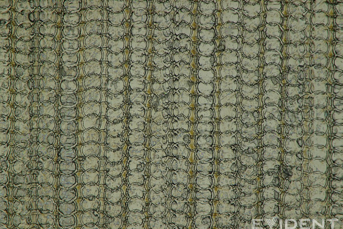
> We tapped in some friends in the additive manufacturing industry, who said it wasn’t quite like any metal 3D printing they’d seen before. Their best guess is that Apple’s using a binder or aerosol jet process in addition to some after-printing machining. I’m curious who they talked to. I’m no expert but this photo [1] looks like laser sintering. It’s got the telltale melt pools and the laser scanning direction from hatch passes Maybe Apple has figured out economic electron beam melting at scale? [1] https://valkyrie.cdn.ifixit.com/media/2025/09/20111617/USBC-... | |||||||||||||||||||||||
| ▲ | noahchen 3 days ago | parent | next [-] | ||||||||||||||||||||||
The video mentions a patent for the 3d printing tech. I think it's this one https://www.patentlyapple.com/2023/08/apple-inherited-a-3d-p... To sum up, it uses an inkjet to spray binder to metal layer by layer. | |||||||||||||||||||||||
| ▲ | dogma1138 3 days ago | parent | prev | next [-] | ||||||||||||||||||||||
This indeed does not look like any sintering MLS or otherwise surface I’ve seen which looks like this https://assets.newatlas.com/dims4/default/0c9b8ea/2147483647... Edit closed surface finish I’ve seen is indeed of a Laser Assisted DED here is a research published this year https://www.sciencedirect.com/science/article/pii/S221486042... | |||||||||||||||||||||||
| |||||||||||||||||||||||
| ▲ | metal_am 3 days ago | parent | prev | next [-] | ||||||||||||||||||||||
Looks like spot melt laser powder bed fusion (L-PBF). Electron beam doesn’t make sense for something on a smaller scale like this; it wouldn't have the resolution. Spot melt is interesting. Renishaw is the only manufacturer I’m aware of that uses a pulsed laser vs continuous wave (and I’m not even sure if they’re still doing that for their newer machines). I would’ve guessed it would’ve been printed on a Farsoon since it’s in China. I just wish the images had scale bars to give a little more info. | |||||||||||||||||||||||
| ▲ | huflungdung 4 days ago | parent | prev [-] | ||||||||||||||||||||||
Those friends could have been managers or sales or HR. Not necessarily engineers. And to save face they are just parroting fab methods they heard in passing. Obviously not DED or binder jetting, and anyone who knows metal printing would see that instantly. DED has the resolution of a hot glue gun, laying down thick beads of molten metal that could never produce such a fine, intricate lattice - it's built for large-scale, rapid deposition, not delicate internal structures. Binder jetting is even more of a non-starter; you're essentially gluing powder together and then sticking it in an oven to sinter. That process leaves behind a distinctly porous, slightly grainy microstructure because the particles are fused, not fully melted, which looks nothing like the smooth, continuous, and fully dense solidified strands you see in this micrograph. This image screams high-precision, localized melting, which is the exclusive domain of powder bed fusion techniques like SLM or DMLS. | |||||||||||||||||||||||
| |||||||||||||||||||||||